
1. Crystal Framework and Split Anisotropy
1.1 The 2H and 1T Polymorphs: Architectural and Electronic Duality
(Molybdenum Disulfide)
Molybdenum disulfide (MoS ₂) is a layered transition metal dichalcogenide (TMD) with a chemical formula including one molybdenum atom sandwiched between two sulfur atoms in a trigonal prismatic sychronisation, developing covalently bound S– Mo– S sheets.
These individual monolayers are piled vertically and held with each other by weak van der Waals forces, making it possible for very easy interlayer shear and exfoliation to atomically slim two-dimensional (2D) crystals– a structural function main to its diverse useful duties.
MoS ₂ exists in numerous polymorphic kinds, the most thermodynamically stable being the semiconducting 2H stage (hexagonal symmetry), where each layer shows a direct bandgap of ~ 1.8 eV in monolayer type that transitions to an indirect bandgap (~ 1.3 eV) wholesale, a sensation essential for optoelectronic applications.
In contrast, the metastable 1T phase (tetragonal symmetry) takes on an octahedral coordination and behaves as a metal conductor as a result of electron donation from the sulfur atoms, allowing applications in electrocatalysis and conductive compounds.
Stage shifts in between 2H and 1T can be generated chemically, electrochemically, or with pressure design, providing a tunable system for designing multifunctional tools.
The capacity to stabilize and pattern these phases spatially within a single flake opens pathways for in-plane heterostructures with distinctive digital domain names.
1.2 Flaws, Doping, and Edge States
The efficiency of MoS ₂ in catalytic and digital applications is extremely conscious atomic-scale issues and dopants.
Innate factor issues such as sulfur jobs act as electron contributors, increasing n-type conductivity and functioning as energetic websites for hydrogen advancement reactions (HER) in water splitting.
Grain limits and line problems can either hamper charge transport or develop localized conductive pathways, relying on their atomic arrangement.
Controlled doping with shift steels (e.g., Re, Nb) or chalcogens (e.g., Se) permits fine-tuning of the band framework, carrier focus, and spin-orbit coupling impacts.
Notably, the sides of MoS ₂ nanosheets, particularly the metal Mo-terminated (10– 10) edges, exhibit substantially higher catalytic activity than the inert basal aircraft, inspiring the layout of nanostructured drivers with made best use of side exposure.
( Molybdenum Disulfide)
These defect-engineered systems exemplify how atomic-level adjustment can change a normally taking place mineral into a high-performance practical material.
2. Synthesis and Nanofabrication Strategies
2.1 Bulk and Thin-Film Production Methods
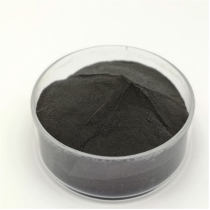
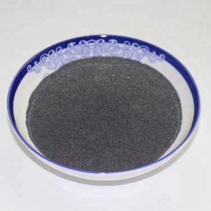
Natural molybdenite, the mineral type of MoS TWO, has been made use of for years as a solid lubricating substance, however modern-day applications require high-purity, structurally managed artificial types.
Chemical vapor deposition (CVD) is the leading approach for creating large-area, high-crystallinity monolayer and few-layer MoS ₂ films on substrates such as SiO ₂/ Si, sapphire, or flexible polymers.
In CVD, molybdenum and sulfur forerunners (e.g., MoO ₃ and S powder) are evaporated at heats (700– 1000 ° C )under controlled ambiences, enabling layer-by-layer development with tunable domain dimension and alignment.
Mechanical exfoliation (“scotch tape method”) remains a benchmark for research-grade samples, generating ultra-clean monolayers with marginal problems, though it does not have scalability.
Liquid-phase exfoliation, entailing sonication or shear blending of bulk crystals in solvents or surfactant services, creates colloidal diffusions of few-layer nanosheets appropriate for coatings, composites, and ink solutions.
2.2 Heterostructure Integration and Tool Pattern
The true potential of MoS two emerges when integrated right into vertical or side heterostructures with various other 2D materials such as graphene, hexagonal boron nitride (h-BN), or WSe two.
These van der Waals heterostructures make it possible for the design of atomically precise devices, consisting of tunneling transistors, photodetectors, and light-emitting diodes (LEDs), where interlayer fee and energy transfer can be crafted.
Lithographic pattern and etching techniques permit the fabrication of nanoribbons, quantum dots, and field-effect transistors (FETs) with network lengths to 10s of nanometers.
Dielectric encapsulation with h-BN secures MoS two from ecological degradation and minimizes charge scattering, considerably boosting service provider movement and gadget security.
These manufacture advances are essential for transitioning MoS ₂ from lab curiosity to feasible element in next-generation nanoelectronics.
3. Practical Qualities and Physical Mechanisms
3.1 Tribological Behavior and Strong Lubrication
One of the oldest and most long-lasting applications of MoS two is as a completely dry strong lubricating substance in extreme environments where liquid oils stop working– such as vacuum, high temperatures, or cryogenic problems.
The reduced interlayer shear toughness of the van der Waals gap enables easy gliding in between S– Mo– S layers, leading to a coefficient of friction as low as 0.03– 0.06 under optimum conditions.
Its efficiency is further enhanced by solid adhesion to steel surface areas and resistance to oxidation up to ~ 350 ° C in air, past which MoO four formation enhances wear.
MoS ₂ is extensively used in aerospace mechanisms, air pump, and weapon elements, typically applied as a layer through burnishing, sputtering, or composite incorporation into polymer matrices.
Recent research studies reveal that humidity can weaken lubricity by raising interlayer attachment, prompting study into hydrophobic coverings or crossbreed lubricants for improved ecological stability.
3.2 Electronic and Optoelectronic Reaction
As a direct-gap semiconductor in monolayer kind, MoS ₂ exhibits strong light-matter communication, with absorption coefficients surpassing 10 ⁵ centimeters ⁻¹ and high quantum yield in photoluminescence.
This makes it perfect for ultrathin photodetectors with quick response times and broadband level of sensitivity, from visible to near-infrared wavelengths.
Field-effect transistors based upon monolayer MoS two show on/off proportions > 10 ⁸ and carrier mobilities up to 500 centimeters ²/ V · s in suspended samples, though substrate interactions typically restrict sensible values to 1– 20 cm TWO/ V · s.
Spin-valley coupling, a consequence of strong spin-orbit interaction and busted inversion proportion, makes it possible for valleytronics– an unique paradigm for info inscribing making use of the valley degree of freedom in momentum space.
These quantum phenomena position MoS two as a candidate for low-power reasoning, memory, and quantum computer elements.
4. Applications in Power, Catalysis, and Emerging Technologies
4.1 Electrocatalysis for Hydrogen Development Response (HER)
MoS ₂ has actually become an appealing non-precious option to platinum in the hydrogen development reaction (HER), an essential procedure in water electrolysis for environment-friendly hydrogen production.
While the basal plane is catalytically inert, side sites and sulfur openings exhibit near-optimal hydrogen adsorption free power (ΔG_H * ≈ 0), comparable to Pt.
Nanostructuring approaches– such as developing up and down straightened nanosheets, defect-rich films, or doped hybrids with Ni or Co– optimize active site thickness and electrical conductivity.
When integrated right into electrodes with conductive sustains like carbon nanotubes or graphene, MoS two attains high existing densities and lasting stability under acidic or neutral problems.
Additional improvement is achieved by maintaining the metal 1T phase, which boosts inherent conductivity and subjects additional active sites.
4.2 Versatile Electronic Devices, Sensors, and Quantum Instruments
The mechanical flexibility, openness, and high surface-to-volume ratio of MoS ₂ make it perfect for flexible and wearable electronics.
Transistors, logic circuits, and memory tools have been shown on plastic substrates, making it possible for bendable displays, health monitors, and IoT sensors.
MoS TWO-based gas sensing units display high level of sensitivity to NO ₂, NH FOUR, and H ₂ O because of bill transfer upon molecular adsorption, with response times in the sub-second variety.
In quantum innovations, MoS two hosts local excitons and trions at cryogenic temperature levels, and strain-induced pseudomagnetic areas can trap service providers, allowing single-photon emitters and quantum dots.
These growths highlight MoS two not just as a functional product yet as a platform for discovering basic physics in reduced measurements.
In recap, molybdenum disulfide exemplifies the merging of timeless materials science and quantum engineering.
From its ancient function as a lubricating substance to its modern-day deployment in atomically slim electronic devices and energy systems, MoS ₂ continues to redefine the limits of what is feasible in nanoscale products style.
As synthesis, characterization, and assimilation techniques breakthrough, its effect throughout science and technology is positioned to expand even additionally.
5. Supplier
TRUNNANO is a globally recognized Molybdenum Disulfide manufacturer and supplier of compounds with more than 12 years of expertise in the highest quality nanomaterials and other chemicals. The company develops a variety of powder materials and chemicals. Provide OEM service. If you need high quality Molybdenum Disulfide, please feel free to contact us. You can click on the product to contact us.
Tags: Molybdenum Disulfide, nano molybdenum disulfide, MoS2
All articles and pictures are from the Internet. If there are any copyright issues, please contact us in time to delete.
Inquiry us