
1. Fundamental Residences and Nanoscale Behavior of Silicon at the Submicron Frontier
1.1 Quantum Confinement and Electronic Structure Transformation
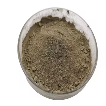
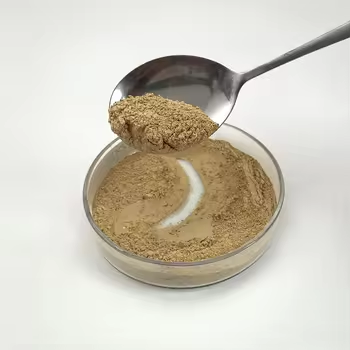
(Nano-Silicon Powder)
Nano-silicon powder, composed of silicon fragments with characteristic measurements listed below 100 nanometers, represents a paradigm shift from mass silicon in both physical behavior and useful utility.
While mass silicon is an indirect bandgap semiconductor with a bandgap of roughly 1.12 eV, nano-sizing generates quantum confinement impacts that basically alter its digital and optical homes.
When the fragment diameter techniques or falls listed below the exciton Bohr radius of silicon (~ 5 nm), cost service providers come to be spatially constrained, leading to a widening of the bandgap and the development of noticeable photoluminescence– a phenomenon absent in macroscopic silicon.
This size-dependent tunability enables nano-silicon to release light throughout the noticeable range, making it a promising prospect for silicon-based optoelectronics, where conventional silicon stops working as a result of its bad radiative recombination effectiveness.
Furthermore, the raised surface-to-volume ratio at the nanoscale boosts surface-related sensations, consisting of chemical reactivity, catalytic task, and interaction with magnetic fields.
These quantum effects are not simply scholastic interests however develop the structure for next-generation applications in energy, sensing, and biomedicine.
1.2 Morphological Variety and Surface Area Chemistry
Nano-silicon powder can be manufactured in different morphologies, consisting of round nanoparticles, nanowires, porous nanostructures, and crystalline quantum dots, each offering distinctive benefits depending on the target application.
Crystalline nano-silicon usually maintains the diamond cubic structure of bulk silicon however exhibits a higher thickness of surface area defects and dangling bonds, which have to be passivated to stabilize the product.
Surface area functionalization– frequently accomplished through oxidation, hydrosilylation, or ligand accessory– plays an essential duty in establishing colloidal security, dispersibility, and compatibility with matrices in compounds or organic atmospheres.
For instance, hydrogen-terminated nano-silicon reveals high reactivity and is vulnerable to oxidation in air, whereas alkyl- or polyethylene glycol (PEG)-layered fragments exhibit enhanced stability and biocompatibility for biomedical usage.
( Nano-Silicon Powder)
The presence of a native oxide layer (SiOₓ) on the particle surface area, even in minimal amounts, significantly affects electrical conductivity, lithium-ion diffusion kinetics, and interfacial responses, particularly in battery applications.
Recognizing and managing surface area chemistry is therefore essential for using the full possibility of nano-silicon in useful systems.
2. Synthesis Strategies and Scalable Construction Techniques
2.1 Top-Down Methods: Milling, Etching, and Laser Ablation
The production of nano-silicon powder can be generally categorized right into top-down and bottom-up approaches, each with distinctive scalability, pureness, and morphological control features.
Top-down strategies include the physical or chemical decrease of mass silicon into nanoscale fragments.
High-energy round milling is a commonly made use of commercial approach, where silicon pieces undergo intense mechanical grinding in inert atmospheres, leading to micron- to nano-sized powders.
While cost-efficient and scalable, this technique usually presents crystal flaws, contamination from grating media, and broad bit dimension circulations, needing post-processing purification.
Magnesiothermic reduction of silica (SiO TWO) complied with by acid leaching is another scalable course, especially when making use of all-natural or waste-derived silica sources such as rice husks or diatoms, supplying a lasting path to nano-silicon.
Laser ablation and reactive plasma etching are much more accurate top-down methods, capable of producing high-purity nano-silicon with regulated crystallinity, however at greater expense and lower throughput.
2.2 Bottom-Up Methods: Gas-Phase and Solution-Phase Growth
Bottom-up synthesis permits greater control over bit dimension, form, and crystallinity by developing nanostructures atom by atom.
Chemical vapor deposition (CVD) and plasma-enhanced CVD (PECVD) make it possible for the development of nano-silicon from aeriform precursors such as silane (SiH FOUR) or disilane (Si two H SIX), with criteria like temperature, stress, and gas circulation dictating nucleation and growth kinetics.
These techniques are particularly effective for generating silicon nanocrystals embedded in dielectric matrices for optoelectronic gadgets.
Solution-phase synthesis, including colloidal courses utilizing organosilicon compounds, permits the production of monodisperse silicon quantum dots with tunable exhaust wavelengths.
Thermal decay of silane in high-boiling solvents or supercritical fluid synthesis likewise produces high-quality nano-silicon with slim size circulations, ideal for biomedical labeling and imaging.
While bottom-up methods usually generate superior material top quality, they encounter obstacles in large-scale production and cost-efficiency, necessitating recurring research into crossbreed and continuous-flow procedures.
3. Energy Applications: Reinventing Lithium-Ion and Beyond-Lithium Batteries
3.1 Duty in High-Capacity Anodes for Lithium-Ion Batteries
One of the most transformative applications of nano-silicon powder depends on energy storage, specifically as an anode product in lithium-ion batteries (LIBs).
Silicon offers a theoretical specific capacity of ~ 3579 mAh/g based upon the development of Li ₁₅ Si Four, which is nearly ten times more than that of conventional graphite (372 mAh/g).
However, the huge quantity expansion (~ 300%) during lithiation triggers bit pulverization, loss of electric contact, and continuous strong electrolyte interphase (SEI) development, bring about fast capability discolor.
Nanostructuring alleviates these concerns by shortening lithium diffusion paths, fitting strain better, and minimizing fracture probability.
Nano-silicon in the kind of nanoparticles, permeable frameworks, or yolk-shell frameworks allows relatively easy to fix cycling with improved Coulombic effectiveness and cycle life.
Commercial battery modern technologies now include nano-silicon blends (e.g., silicon-carbon composites) in anodes to enhance energy thickness in consumer electronic devices, electric lorries, and grid storage systems.
3.2 Potential in Sodium-Ion, Potassium-Ion, and Solid-State Batteries
Past lithium-ion systems, nano-silicon is being explored in emerging battery chemistries.
While silicon is much less reactive with salt than lithium, nano-sizing boosts kinetics and allows minimal Na ⁺ insertion, making it a candidate for sodium-ion battery anodes, specifically when alloyed or composited with tin or antimony.
In solid-state batteries, where mechanical stability at electrode-electrolyte interfaces is essential, nano-silicon’s ability to undertake plastic deformation at small scales reduces interfacial tension and enhances get in touch with maintenance.
Additionally, its compatibility with sulfide- and oxide-based strong electrolytes opens up opportunities for much safer, higher-energy-density storage space services.
Research continues to maximize user interface engineering and prelithiation approaches to make best use of the long life and performance of nano-silicon-based electrodes.
4. Arising Frontiers in Photonics, Biomedicine, and Compound Materials
4.1 Applications in Optoelectronics and Quantum Light
The photoluminescent buildings of nano-silicon have rejuvenated initiatives to create silicon-based light-emitting gadgets, a long-standing obstacle in integrated photonics.
Unlike mass silicon, nano-silicon quantum dots can display reliable, tunable photoluminescence in the noticeable to near-infrared range, enabling on-chip source of lights compatible with complementary metal-oxide-semiconductor (CMOS) innovation.
These nanomaterials are being incorporated into light-emitting diodes (LEDs), photodetectors, and waveguide-coupled emitters for optical interconnects and noticing applications.
In addition, surface-engineered nano-silicon exhibits single-photon discharge under specific flaw setups, placing it as a possible platform for quantum information processing and safe and secure communication.
4.2 Biomedical and Environmental Applications
In biomedicine, nano-silicon powder is getting focus as a biocompatible, eco-friendly, and safe option to heavy-metal-based quantum dots for bioimaging and medication delivery.
Surface-functionalized nano-silicon particles can be created to target certain cells, release therapeutic agents in reaction to pH or enzymes, and offer real-time fluorescence tracking.
Their destruction into silicic acid (Si(OH)FOUR), a naturally taking place and excretable substance, reduces long-lasting poisoning problems.
Additionally, nano-silicon is being explored for ecological remediation, such as photocatalytic deterioration of contaminants under visible light or as a minimizing representative in water therapy procedures.
In composite products, nano-silicon boosts mechanical toughness, thermal security, and wear resistance when included into steels, porcelains, or polymers, particularly in aerospace and automotive components.
Finally, nano-silicon powder stands at the junction of basic nanoscience and industrial innovation.
Its unique combination of quantum results, high sensitivity, and versatility throughout power, electronics, and life scientific researches highlights its function as an essential enabler of next-generation modern technologies.
As synthesis techniques development and combination obstacles are overcome, nano-silicon will certainly remain to drive progress toward higher-performance, sustainable, and multifunctional product systems.
5. Vendor
TRUNNANO is a supplier of Spherical Tungsten Powder with over 12 years of experience in nano-building energy conservation and nanotechnology development. It accepts payment via Credit Card, T/T, West Union and Paypal. Trunnano will ship the goods to customers overseas through FedEx, DHL, by air, or by sea. If you want to know more about Spherical Tungsten Powder, please feel free to contact us and send an inquiry(sales5@nanotrun.com).
Tags: Nano-Silicon Powder, Silicon Powder, Silicon
All articles and pictures are from the Internet. If there are any copyright issues, please contact us in time to delete.
Inquiry us